What are perovskite quantum dots?
What are perovskite materials?
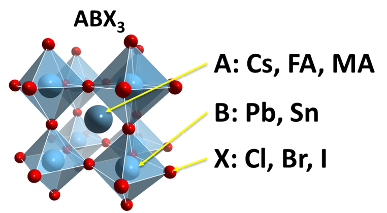
In materials science and optoelectronics, perovskite materials drew a lot of attention due to their unique performance in solar cells, lighting, displays, catalysis and many other areas. The term perovskite refers to a calcium titanium oxide mineral, with the chemical formula CaTiO3. The terms “perovskite” and “perovskite structure” are often used as if they were interchangeable, whereas in reality true perovskite (the mineral) is composed of calcium, titanium, and oxygen in the form CaTiO3 and a perovskite structure is anything that has the generic form ABX3 and the same crystallographic structure as perovskite (the mineral). In a perovskite structure, ‘A’ and ‘B’ are two cations of very different sizes, and X is an anion that bonds to both. Gustav Rose discovered perovskite in the Russian Ural Mountains in 1839 and named it after Russian mineralogist Lev Perovski (1792–1856). Many different cations can be embedded in this structure, which makes it possible to develop diverse engineered materials.
For optoelectronics, halide perovskite materials are of particular interest. In these materials, the perovskite structure ABX3 is formed by octahedral, with halogens on the corner (X: Cl, Br or I); transition metals in the centre (B: Pb or Sn) and cations in between octahedral (A: Cs, organic FA (formamidinium CH(NH2)2) or MA (methylammonium CH3NH3)). These semiconducting materials have a unique combination of optical properties, such as direct and tuneable bandgaps, high absorption coefficients, broad absorption spectra, high charge carrier mobilities, long charge diffusion lengths and remarkably low trap densities. They are considered as rising stars of the photovoltaic industry. They are cheap and easy to manufacture, and extremely effective. That is why they have been widely investigated for use in solar cells, lasing, light-emitting diodes and photodetectors.
How do perovskite materials relate to the quantum dot industry?
A new class of quantum dots, based on perovskite semiconducting materials, is currently under development. As the size of the halide perovskite crystals decreases and reaches a scale of nanometres, they start to exhibit quantum confinement and demonstrate photoluminescence. These nanocrystals (quantum dots) possess outstanding photoluminescence efficiency of up to 100 % (the photoluminescence quantum yield, or PLQY, of a molecule or material is defined as the number of photons emitted as a fraction of the number of photons absorbed). They also have high colour purity (characterised with the emission full width at half maximum (FWHM) and usually is 20-35 nm that is the best among all quantum dots), and a high absorption coefficient. These materials demonstrate superb light photo- and electrical- conversion and are promising for applications in displays, UV and X-ray sensors, and lighting devices. They have a greater tolerance to imperfections than metal chalcogenide quantum dots, and they have excellent quantum yields of photoluminescence and high colour purity that have already surpassed metal chalcogenide QDs.
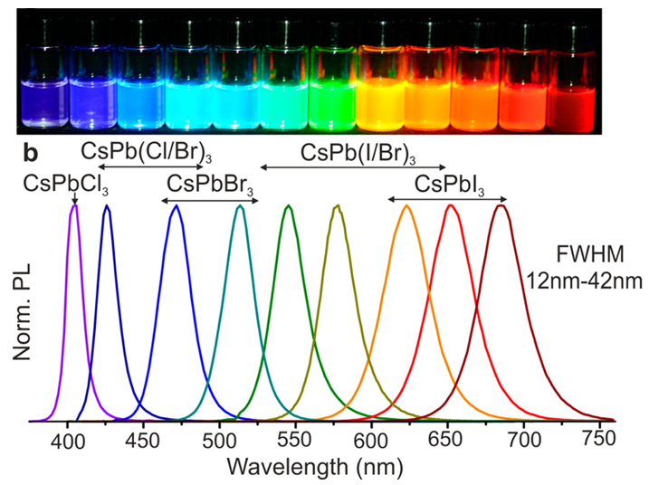
While perovskite quantum dots behave similarly to traditional chalcogenide quantum dots, there are some differences. The main difference is that while in chalcogenide quantum dots the tuning of the bandgap (or colour of the emitted light) is done by changing quantum dots’ size (for example 6 nm CdSe QDs emit red light, 3 nm – green light and 2 nm – blue light), in perovskite QDs the tuning of the emitting light is performed by changing of perovskite QDs composition. Pure CsPbCl3 QDs emit the light in UV range, CsPbBr3 QDs emit green light and CsPbI3 emit red light. The most exciting part is that you can make perovskite QDs emit light in any colour by tuning their halide composition. For example, if you start to add bromide ions to the CsPbCl3 QDs, this results in the partial replacement of the chloride ion with the bromide ion CsPb(Cl/Br)3. Thus, the light emitted will gradually shift from being blue and sky blue to being green when the bromide has completely replaced the chloride ions. This results in the CsPbBr3 structure. By adding iodide ions to green emitting CsPbBr3 QDs, it is possible to go all the way from having yellow and orange light emission from CsPb(Br/I)3 to having deep red light from CsPbI3.
But, is it possible to change the bandgap (in other words the colour of the emitted light) by changing the perovskite nanocrystal size? Well, it is possible, but only to a certain extent. For example, if the size of CsPbBr3 is reduced from 12 nm to 1 nm, the bandgap only changes from 2.4 eV (515 nm) to 2.9 eV (430 nm), or on average 0.05 eV/nm. But for CdSe QDs, the size change from 6 nm to 2 nm results in a bandgap change from 2.0 eV (630 nm) to 2.7 eV(460 nm) – on average 0.18 eV/nm. In case of PbS QDs, the change of the size from 9 nm to 2.2 nm results in the bandgap changing from 0.6 eV (2050 nm) to 1.46 eV (850 nm) – on average 0.13 eV/nm. Therefore, it can be seen that the bandgap in perovskite QDs is 3-5 times less sensitive to the nanocrystal size change than in traditional quantum dots. The big advantage of this is that the optical properties of perovskite QDs are more reproducible from batch to batch in their synthesis. It is possible to scale up the production in large volumes, maintaining precise control of emission peaks (±1-3 nm) and achieving the best colour purity (FWHM < 18-20 nm).
An additional advantage of perovskite QDs over traditional quantum dots is that they are highly tolerant to imperfections, since they do not require any surface passivation (passivation is the process of treating or coating a metal in order to reduce the chemical reactivity of its surface) to retain their high PLQY. If there are any defect and trap locations on the surface, their energies are positioned beyond the bandgap and are either located inside the conduction or valence bands and less (weakly) affect into the QDs optical properties. Such properties are highly desirable for electronic and optoelectronic applications. The perovskite material nanocrystals are easy to synthesise in a colloidal suspension, and are also easily incorporated into optoelectronic devices using readily available processing techniques. This makes them a powerful potential contributor to future technologies in next generation LCD and OLED displays, photodetectors, and solar cells.
Perovskite quantum dot applications
Perovskite quantum dots are less well researched than other types of quantum dots, as they were first reported in 2015. However, thus far, perovskite quantum dots have proven extremely effective in optoelectronics and nanotechnology for a variety of different applications. Potential applications for perovskite quantum dots include:
- X-Ray and UV Image Sensors
- Displays
- Light Emitting Diodes
- Lasers
- Solar Cells
- Single Photon Sources
- Quantum Computing
- Cell imaging
X-Ray and UV Image Sensors
Perovskite QDs exhibit outstanding luminescence under exposure to high energy photons, such as Perovskite QDs exhibit outstanding luminescence under exposure with high energy photons, such as X-rays or UV light. This can be used in image sensor devices, where QDs are used as a scintillation material to convert high energy photons to visible light that can be captured by commercially available silicon sensors. Quantum Dot X-ray and UV sensing technologies are brand new and research is still ongoing.
Displays
Green emitting perovskite QDs QDs can be successfully used as a light down-converting material in LCD backlighting, or OLED colour filters where QDs convert the blue light into green light by photoluminescence. Due to Perovskite QDs’ high PLQY (up to 100%) and high colour purity (FWHM <20-25 nm), they are a better-quality alternative to the current green CdSe or InP based QDs. Perovskite QDs can enhance the colour gamut in displays, achieving > 85% of Rec.2020 colour standard coverage, meaning that displays present more vibrant and vivid colours in TVs, laptops and tablets. The first commercially available display with Perovskite QDs is expected to appear on the market in 2021
Light-emitting Diodes
Due to their high electroluminescent efficiency, perovskite materials may be good candidates for use in light-emitting diodes (LEDs). In this application, perovskite QDs convert the electric current into light with high colour purity and brightness. This will be an invaluable solution for flexible and curved displays in TVs, mobile and wearable devices, virtual and augmented reality glasses, automotive displays and signage. Today, QDLED blue devices can achieve an external quantum efficiency of 12.3% and the green devices achieve an external quantum efficiency of 22 %, with brightness > 1000 Cd/m2 . Since these perovskite QDLEDs have limited durability, this application of QDs is still at the R&D stage.
Lasers
Lead halide perovskite nanocrystals (NCs) have garnered recent attention because of their unique versatility as laser gain materials. The main advantage of Perovskite QDs is their high PLQY of up to 100% and their high tolerance to imperfections. Different structures of lasers can be achieved with perovskite QDs, especially with CsPbBr3 QDs. These include WGM, VCSEL, DBR, DFB, random cavity, and film only, with ultralow lasing thresholds (as low as 0.39 μJ/cm2).
Conclusion
Perovskite materials are extremely promising in the advanced optoelectronic industry. For instance, perovskite materials have demonstrated extensive potential in displays, photodetectors, lasing, photovoltaic devices, and even in other applications. The combination of their unique properties makes them useful in real-world applications for the benefit and service of humankind.
Useful links:
https://pubs.acs.org/doi/10.1021/nl5048779
https://www.ncbi.nlm.nih.gov/pmc/articles/PMC5872950/
https://www.sciencedirect.com/science/article/pii/S2090997714000212
https://www.nature.com/articles/s41586-018-0451-1?proof=t
https://www.nature.com/articles/s41377-019-0204-4