Why InAs Quantum Dots?
Unlocking the Potential of InAs Quantum Dots: Pioneering the Future of SWIR Technology
Quantum dots (QDs) have emerged as remarkable materials due to their tunable electronic and optical properties. By varying their composition or size, it is possible to engineer their band gap according to specific requirements. Quantum dots with emissions in the visible range, such as those based on CdSe or InP, have been widely used for color conversion in displays and LED lights. Their narrow photoluminescence (PL) width enables displays to render true and realistic colors.
Beyond the visible range, QDs have been extensively studied for applications in photovoltaics, infrared photodetectors, and image sensors. For instance, in infrared image sensors, QDs can reduce manufacturing costs thanks to their scalable, solution-processable techniques, compared to the conventional vacuum deposition methods used for epitaxially grown InGaAs image sensors. Recently, PbS QDs have been utilized in SWIR (Short Wave Infrared: 1-3µm range) cameras, offering a broader spectral range of up to 2000 nm compared to standard InGaAs cameras. In some applications, such as consumer electronics, the use of QDs containing heavy metals, such as Pb or Cd, is regulated by RoHS (restrictions of hazardous substances) regulations. This regulation underscores the importance of developing heavy metal-free QDs for the SWIR range. Reducing production costs will promote the use of SWIR technology in consumer electronic products. Among the various types of heavy metal-free QDs available for the SWIR range, InAs QDs holds significant potential to advance QD SWIR technology.
Understanding InAs Quantum Dots
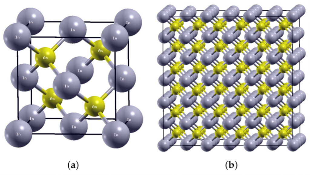
InAs quantum dots are semiconductor nanoparticles composed of Indium (In) and Arsenic (As) atoms, classified as III-V semiconductors. Among III-V materials, InAs exhibits three times higher electron mobility compared to InGaAs or GaAs. InAs has a zinc-blende structure with a lattice constant of 6.05 Å. The In-As bonds have a Phillips Ionicity of 0.36, which is much lower compared to other semiconductors, such as Pb-S (PI = 0.70) or Cd-Se (PI = 0.77). This lower ionicity indicates that InAs has more covalent bonding, contributing to its structural stability. Consequently, growing high-crystallinity QDs requires higher temperatures, typically exceeding 240-300°C. The resulting QDs are usually stable under elevated conditions up to 200-250°C.

Optical and Electronic Properties
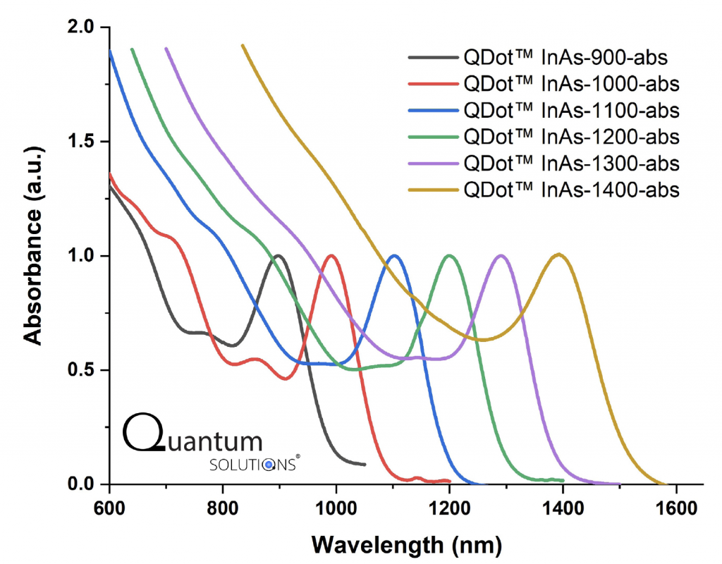
Due to quantum confinement, InAs QDs possess a tunable bandgap, allowing researchers to manipulate their absorption and emission spectra across a wide range of wavelengths from the near-infrared (NIR) to short-wave infrared (SWIR). As InAs QDs have more covalent bonds, they are expected to have a large exciton Bohr radius, enabling size-dependent optical properties to be observed in relatively large particles. The exciton Bohr radius is reported to be around 31 nm to 45 nm. The size of InAs quantum dots dictates their optical and electronic properties. As shown in Figure 2 below, the larger the size of the InAs QDs, the absorbance shifts to higher wavelengths (red-shifted): from 900 nm for 3 nm particles to 1400 nm for 7 nm particles.

InAs QDs application
The tunability of optical and electronic properties of InAs QDs makes them promise in various applications, for example including but not limited to:
SWIR photodetectors and image sensor
InAs QDs can enable solution processable manufacturing and reduces the overall cost of the SWIR photodetectors and image sensors. InAs quantum dots are the most promising candidates for Pb-free materials for these devices, addressing the demand for SWIR sensors in consumer electronics. Additional benefits include their high thermal stability (up to 200-250°C) and fast response time in the sub-nanosecond range, making them suitable for LIDAR applications. These sensors may find promise in applications such as mobile phones (phase recognition, biometrics) or automotive systems (improving visibility in degraded weather conditions such as fog or rain).
Biomedical Imaging
InAs QDs have garnered significant interest in biomedical imaging applications. Their narrow and tunable emission spectra in the SWIR range make them excellent candidates for fluorescence labeling and deep tissue bioimaging applications, particularly at wavelengths around 1200 nm and 1600 nm, where there is minimal water absorption and the skin becomes transparent.
Optical Communication
Wavelengths around 1310 nm and 1550 nm are very important for undersea and long-distance optical communication due to low attenuation in fiber optics and low interference with atmospheric conditions. InAs QD photodetectors can be used as receivers in these fiber optic communication systems, as they have been reported to have fast (sub ns) response times.
Quantum Communication and Computation
InAs QDs hold immense promise in the field of quantum information technologies. InAs QDs are a promising platform for single-photon emission and can be integrated with various photonic elements for quantum communication applications.
In conclusion, InAs quantum dots represent a versatile and promising material due to their tunable electronic and optical properties. Their ability to adjust the bandgap through changes in particle size makes them suitable for SWIR photodetectors and image sensors. InAs QDs offer significant advantages, including high electron mobility, structural stability, thermal resilience, and fast response times. Moreover, the potential of InAs QDs to operate within the SWIR range without heavy metals addresses regulatory concerns and paves the way for their integration into consumer electronics. As research continues, the unique characteristics of InAs QDs are poised to revolutionize multiple industries, highlighting their pivotal role in the future of imaging and sensing.
About Quantum Solutions:
Quantum Solutions develops revolutionary beyond-visible imaging solutions that give affordable access to spectra of light which the naked eye is incapable of perceiving: shortwave infrared, midwave infrared, and X-rays. The sensors are based on our revolutionary quantum dots materials. Contact us at [email protected] to discuss your needs for enabling the next generation of imaging systems using QDot™ InAs quantum dots.
