Q.Eye® SWIR photodetectors
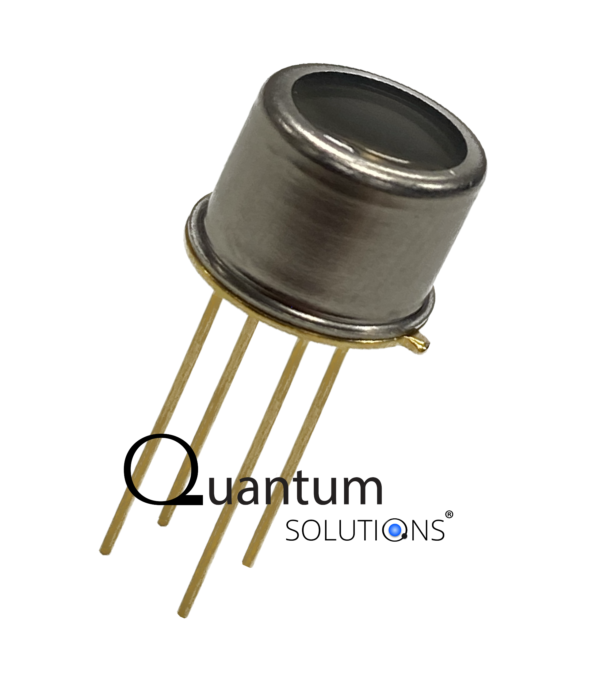
Q.Eye® SWIR photodetectors are a collection of evaluation samples of single-pixel quantum dot photodetectors that operate from visible (400 nm) to short-wave infrared (SWIR) range, with variable cut-off wavelengths ranging from 900 to 2500 nm. In contrast to traditional infrared (IR) sensors, quantum dot sensors exhibit specific absorption profiles that are tuned by the quantum dot sizes used, ranging from 2 nm to 12 nm, thereby adjusting the absorption cut-off from 900 to 2500 nm. The sensor’s characteristic profiles exhibit peaks at wavelengths characteristic to the size of the employed quantum dots. Initial evaluation samples come with 5.6 nm size quantum dots that feature an absorbance peak at 1450 nm. Another wavelength ranges available upon request. The active area size is 0.1 mm x 0.1 mm, and other configurations (up to 3 mm) can also be accommodated upon request. The photodiode comes on a wafer die with the size 3 x 3 mm. TO5 packaged photodiode is available for easier testing and evaluation.
Q.Eye® SWIR photodetectors are a collection of evaluation samples of single-pixel quantum dot photodetectors that operate from visible (400 nm) to short-wave infrared (SWIR) range, with variable cut-off wavelengths ranging from 900 to 2500 nm.
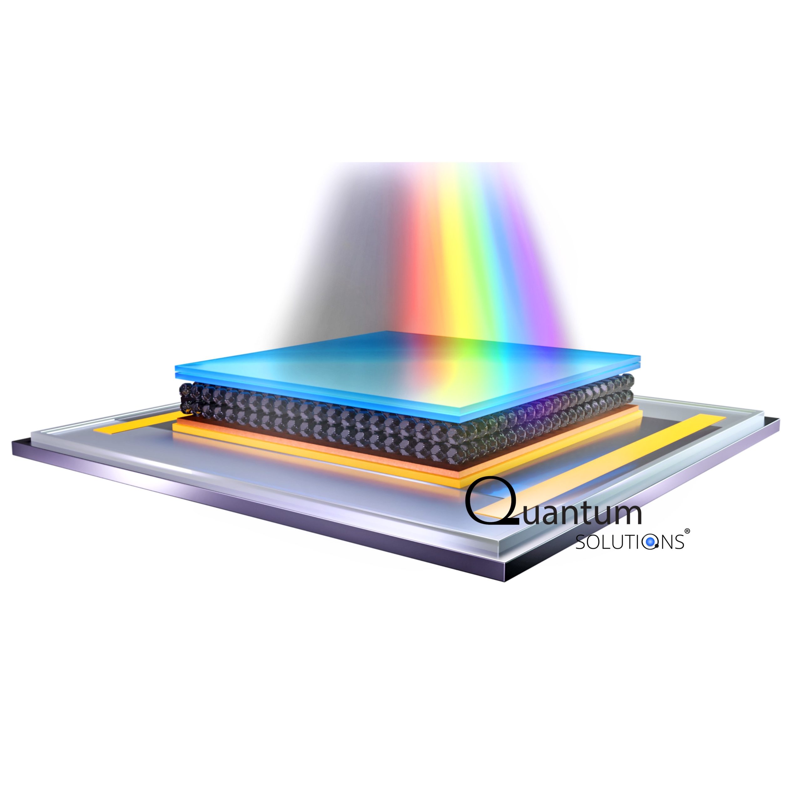
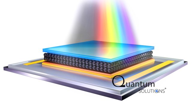
The main distinction between quantum dot photodiodes and traditional infrared (IR) sensors, such as PbS, PbSe, or InGaAs, lies in their processing methods. Quantum dot photodetectors are solution-processed and monolithically integrated on a silicon CMOS substrate, offering the advantage of being producible on large silicon CMOS wafers of 150 mm, 200 mm, or larger. This characteristic renders them economically viable for low-cost and large-scale applications, such as wearables, mobile devices, automotive systems, and more. In contrast to traditional IR sensors, quantum dot sensors exhibit specific absorption profiles that are tuned by the quantum dot sizes used, ranging from 2 nm to 12 nm, thereby adjusting the absorption cut-off from 900 to 2500 nm. The sensor’s characteristic profiles exhibit peaks at wavelengths characteristic to the size of the employed quantum dots.
Initial evaluation samples feature an absorbance peak at 1450 nm. Other wavelength ranges available upon request. The active area size is 0.1 mm x 0.1 mm, and other configurations (up to 3 mm) can also be accommodated upon request. The photodiode comes on a wafer die with the size 3 x 3 mm. TO5 packaged photodiode is available for easier testing and evaluation. The photodetector architecture is depicted below:
Q.Eye® SWIR photodetectors offer the following advantages:
- Solution-processed compound semiconductor SWIR sensors, monolithically integrated on silicon CMOS substrates, ensuring a compact design, an economical price, and the potential for mass production.
- These sensors exhibit excellent sensitivity and offer the potential to fine-tune the balance between sensitivity and dark current.
- The design is tunable, allowing for absorbance across a range from 900 to 2500 nm and active area from 0.1 mm x 0.1 mm to 3 mm x 3 mm, even more.
Click here to download the Technical Specification for detailed information.
Q.Eye® is a trademark of QUANTUM SOLUTIONS. Contact us to make any requests and questions or buy products.
