-
2025
-
2024
-
Nov262024Q.Cam™ Product Release
-
Sep192024Q.Fly Product Release
-
Jul232024TOPODRONE and QUANTUM SOLUTIONS announce Collaboration on Next-Generation VIS-SWIR Camera for UAV Platforms
-
May212024Quantum Solutions Presented at CLEO 2024
-
Apr162024Quantum dot short-wave infrared (SWIR) image sensors sales release
-
Feb122024200 mm wafer level processing of QDot™ quantum dot n-type ink
-
Jan312024Sales Release of QDot™ CsPbBr3 Perovskite Single Crystals
-
-
2023
-
Dec202023Sales Release of Large Sise QDot™ InAs Quantum Dots
-
Oct242023Quantum Solutions Presented at Phosphors & Quantum Dots Industry Forum 2023 in Seoul
-
Oct102023Sales Release of Q.Eye™ SWIR Photodetectors
-
Oct042023Nobel Prize for the groundbreaking research in quantum dots
-
Oct012023Sales Release of QDot™ Perovskite Single Crystals
-
Sep302023Sales Release of QDot™ PbS quantum dot n-type ink
-
Jun152023Sales Release of QDot™ InAs Quantum Dots
-
Jun072023Sales Release of QDot™ ETL and HTL for SWIR image sensors
-
-
2022
-
2021
Perovskite single crystals demonstrating record-high performance in direct X-ray detection
Oxford, UK – January 13, 2025 - AY Sensors and Quantum Solutions have demonstrated record-high performance of perovskite single crystals for next-generation direct X-ray and gamma-ray detectors.
AY Sensors and Quantum Solutions are thrilled to announce the achievement of record-high performance for their product, QDot™ CsPbBr₃ perovskite single crystals, in X-ray detection. Direct X-ray sensors were fabricated through the monolithic integration of single crystals onto the substrate using a solution processing technique. The detectors exhibited exceptional linearity (R2 = 0.9995) across a wide X-ray dose range (0.08 to 33.60 μGyairs–1), achieving sensitivity over 2,000 μCGyair–1 cm–2 at low bias, a detection limit of 11 nGyairs–1 at 10V, and MTF > 0.5 at 3 lp mm-1. [1]
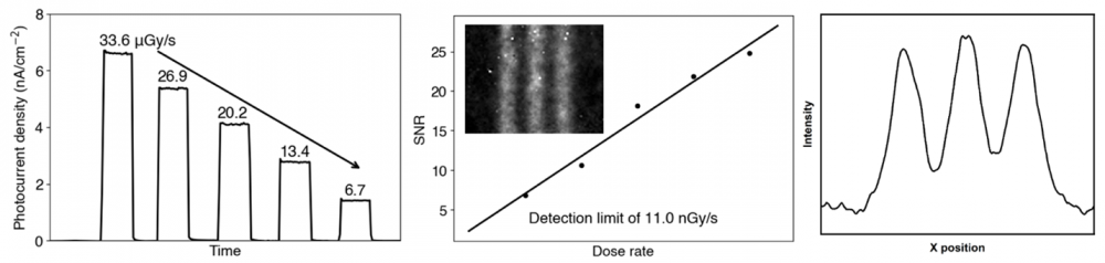 CsPbBr₃ X-ray detector and image-sensor performance characteristics. Left: Photocurrent as a function of X-ray dose rate, middle: SNR as a function of X-ray dose rate (inset: X-ray image of a 3 lp mm-1 line pair gauge), right: Profile plot of a 3 lp mm-1 line pair gauge image.
In comparison, current state-of-the-art CZT (cadmium zinc telluride) based direct detectors demonstrated X-ray sensitivity around 1600 μC·Gyair-1 cm-2 [2]. The combination of high performance and low-cost integration of QDot™ CsPbBr₃ single crystals on readout chips has the potential to disrupt current direct X-ray detection technology, making high-performance medical imaging and computed tomography more accessible. The ability of perovskite single crystals to bond easily with both rigid and flexible circuits, along with their compatibility with ASIC/CMOS technology, opens up new avenues for using these detectors in medical, security, and inspection imaging and sensing.
This collaborative breakthrough is the result of combining AY Sensors' expertise in solution-grown perovskite single crystals with Quantum Solution’s cutting-edge sensor fabrication technology, offering a cost-effective alternative to traditional CZT-based X-ray and gamma-ray detection technology.
QDot™ single crystals are grown from solution, with sizes ranging from 5x5x1.5 mm3 to 50x50x15 mm3. Their high electron and hole mobility make them ideal for a wide range of applications requiring high sensitivity, reproducibility, and stable performance.
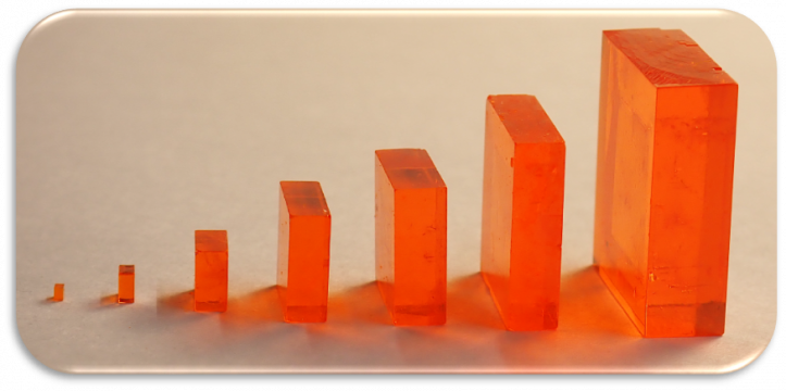 Solution-grown perovskite Single Crystals of various sizes by AY sensors.
Key Features of QDot™ Single Crystal:
• Exceptional Crystallinity: The full width at half maximum (FWHM) of the rocking curve peak in the X-ray diffractometer (XRD) spectrum is less than 100 arcseconds (arcsec), indicating high-quality crystal formation.
• High Sensitivity: The high atomic number of lead (Pb) in perovskite crystals contributes to efficient photon interaction, making QDot™ Single Crystals highly sensitive to X-ray and gamma-ray radiation.
• Large Crystal Growth: Larger crystals reduce the number of grain boundaries, improving overall detector performance and reliability.
• Low-Temperature Processing: This feature enables the integration of perovskite detectors with a broader range of materials and substrates.
• Cost-Effective Manufacturing: The solution-based fabrication process of Perovskite Single Crystals is more cost-effective compared to traditional, complex, and expensive crystal growth methods.
• Direct Bonding to readout chips: Perovskite Single Crystals can be directly bonded to a readout chip by solution processing techniques without the need for pixelating the crystal or bond-to-bond connections.
• Reduced Dead Area Between Crystals: The smaller dead area between crystals allows for seamless integration, enhancing image quality when the crystals are placed on a PCB board.
QDot™ Single Crystals are designed for industries that require high sensitivity, fast response time, reliable, and reproducible devices for X-ray imaging and gamma-ray spectrometry, including:
• Medical Imaging
• Computed Tomography
• Radiation Protection
• Nuclear Spectroscopy
• Gamma Spectroscopy
Stay Tuned for More: For any inquiries or to schedule a meeting, feel free to contact AY Sensors at [email protected] and Quantum Solutions at [email protected].
About AY Sensors: AY Sensors is transforming the medical imaging industry by developing high-quality perovskite single crystals for X-ray and gamma-ray detectors, making advanced diagnostics more accessible and affordable globally. Contact us at [email protected] to discuss your needs for the next generation of single crystal solutions.
About Quantum Solutions: Quantum Solutions specializes in the development and manufacturing of X-ray image sensors using perovskite single crystals, enabling high-resolution image capture. This includes custom-designed, low-power silicon readout integrated circuit (ROIC) chips for X-ray image processing. Contact us at [email protected] to explore your needs for next-generation imaging systems.
[1] https://pubs.acs.org/doi/full/10.1021/acsmaterialslett.4c01039
[2] https://www.osti.gov/servlets/purl/1873520
Previous publications
