-
2025
-
Oct102025Introducing Q.Fly® Solar at Solar & Storage Live 2024
-
Sep012025Quantum Solutions Showcased at Commercial UAV Expo 2024
-
Jan132025Perovskite single crystals demonstrating record-high performance in direct X-ray detection
-
Jan132025Re-introducing Q.Fly™ – Now Available with Academic and Research Discounts
-
-
2024
-
Nov262024Q.Cam™ Product Release
-
Sep192024Q.Fly Product Release
-
Jul232024TOPODRONE and QUANTUM SOLUTIONS announce Collaboration on Next-Generation VIS-SWIR Camera for UAV Platforms
-
May212024Quantum Solutions Presented at CLEO 2024
-
Apr162024Quantum dot short-wave infrared (SWIR) image sensors sales release
-
Feb122024200 mm wafer level processing of QDot™ quantum dot n-type ink
-
Jan312024Sales Release of QDot™ CsPbBr3 Perovskite Single Crystals
-
-
2023
-
Dec202023Sales Release of Large Sise QDot™ InAs Quantum Dots
-
Oct242023Quantum Solutions Presented at Phosphors & Quantum Dots Industry Forum 2023 in Seoul
-
Oct102023Sales Release of Q.Eye™ SWIR Photodetectors
-
Oct042023Nobel Prize for the groundbreaking research in quantum dots
-
Oct012023Sales Release of QDot™ Perovskite Single Crystals
-
Sep302023Sales Release of QDot™ PbS quantum dot n-type ink
-
Jun152023Sales Release of QDot™ InAs Quantum Dots
-
Jun072023Sales Release of QDot™ ETL and HTL for SWIR image sensors
-
-
2022
-
2021
200 mm wafer level processing of QDot™ quantum dot n-type ink
Quantum Solutions demonstrated the 200 mm wafer level processing of QDot™ quantum dot n-type ink
[Southampton, 12.02.2024] — Quantum Solutions is pleased to announce the successful demonstration of wafer-level deposition of QDot™ PbS quantum dot n-type ink on a 200 mm silicon ROIC (read-out integrated circuit) wafer. This groundbreaking work highlights the feasibility of producing SWIR (short-wave infrared) image sensors with high throughput on 200 mm wafer platforms, essential for large-scale manufacturing of sensors.
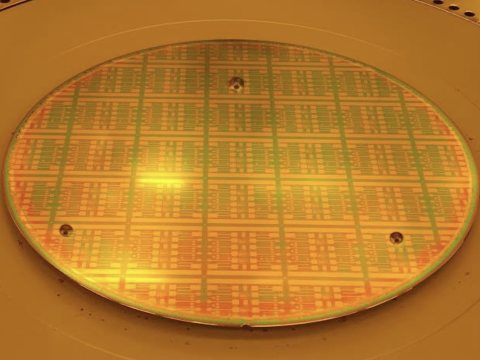
The QDot PbS n-type ink was efficiently introduced into the 200 mm imec FAB for a single-step spin-coating process. The single-step deposition of the ink was executed seamlessly over the 200mm wafer, achieving a thickness range of 50-100 nm depending on the spin-coating speed parameters. The resulting thin films were smooth and free of noticeable defects, with less than 4% thickness variation observed across the 200 mm wafer:

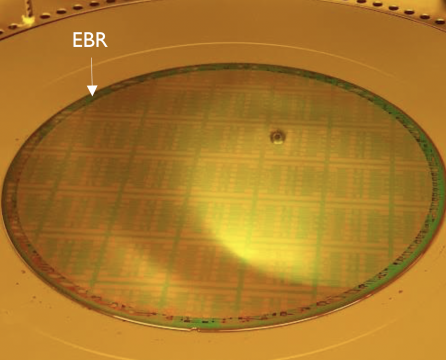
Additionally, multistep coating of thicker films up to 200-300 nm was verified. Furthermore, we successfully implemented Edge Bead Removal (EBR) technique on the wafer:

Quantum Solutions' QDot™ PbS quantum dot n-type ink (n-ink) is specifically designed for manufacturing high-efficiency SWIR (short-wave infrared) photodiodes and image sensors. This ink streamlines the solution-processing fabrication flow of quantum dot SWIR sensors by eliminating the need for complex solid ligand exchange procedures. The ink also facilitates cost-effective production because it requires a smaller volume for coating large wafers, comparable to multistep solid ligand exchange process. This makes it a practical choice for scaling up production of SWIR photodiodes and image sensors. For more details, please contact us at [email protected].
About Quantum Solutions:
Quantum Solutions develops and manufactures quantum dot “wide-range” sensors and materials for “superhuman” vision, enabling the capture of images invisible to the naked eye. This includes lower-energy SWIR and MWIR spectrums, as well as higher-energy UV and X-ray light ranges. Cameras equipped with these sensors can find numerous applications across various fields, including robotics, machine vision, the automotive industry, security, and consumer electronics. We envision a future where cameras with augmented vision become the standard in our world. Contact us at [email protected] to discuss your needs for enabling the next generation of imaging systems.
###
Previous publications

