QDot™ ETL and HTL materials
Quantum Solutions provides a library of QDot™ ETL and HTL materials that can be used together with SWIR QDot™ quantum dots, enabling the fabrication of highly efficient short-wave infrared (SWIR) photodiodes and image sensors. QDot™ ETL and HTL materials offer the following features:
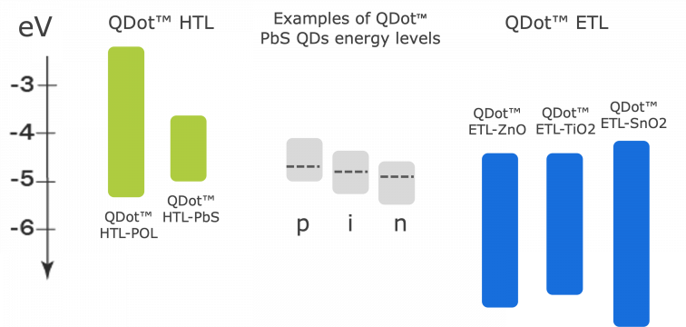
- Carefully designed electronic landscape of ETL and HTL semiconducting materials providing a perfect band alignment with SWIR QDot™ quantum dot absorbers. Suitable energy levels can be selected from the library of available materials or fine-tuned upon request.
- Easy to process on substrates (glass, silicon or CMOS wafers) by spin-coating or other printing processes, guaranteeing affordability, manufacturability and economical price (10 mL is sufficient for one or two 200 mm wafers).
- Enhanced functionality, stable operation, and long-term environmental durability.
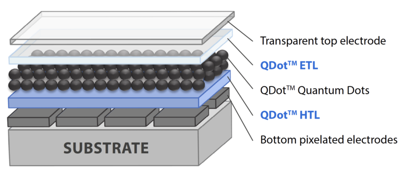
Quantum Solutions offers a range of materials for fabricating a QDot™ photodiode stack, which can be used in sensing and imaging applications. The principal device structure comprises several thin layers, referred to as a QDot™ stack, placed on top of a substrate. Working from the bottom up, the structure includes a bottom electrode, an HTL (hole transport layer), a quantum dots absorber, an ETL (electron transport layer), and a transparent top electrode.
QDot™ stack materials, including HTL, quantum dots, and ETL, can be deposited onto any target substrate, such as glass, silicon, or a ROIC platform, using spin-coating methods from solution.
These novel solution-based methods for depositing thin films of compound semiconductor materials have made it possible to create artificial nanocrystalline structures that offer unprecedented possibilities. Unlike epitaxial layers, the quality of quantum-dot semiconductors is less dependent on the crystallographic characteristics of substrates and their interfacial relationships. Solution-based methods provide flexibility and broad material choice for specialised carrier transport layers enabling tuneable photodiode functions.
Quantum Solutions provides a library of QDot™ ETL and HTL materials that can be used together with SWIR QDot™ quantum dots, enabling the creation of highly efficient SWIR photodiodes and image sensors. QDot™ ETL and HTL materials offer the following features:
- Carefully designed electronic landscape of ETL and HTL semiconducting materials providing a perfect band alignment with QDot™ PbS quantum dot absorbers. Suitable energy levels can be selected from the library of available materials or fine-tuned upon request.
- Easy to process on substrates (glass, silicon or CMOS wafers) by spin-coating or other printing processes, guaranteeing affordability, manufacturability and economical price (10 mL is sufficient for one or two 200 mm wafers).
- Enhanced functionality, stable operation, and long-term environmental durability.
Click here to view the Technical Specification for detailed information.
QDot™ is a trademark of QUANTUM SOLUTIONS. Contact us to make any requests and questions or buy products online