Quantum Dot VIS-SWIR cameras
1. Application areas for VIS-SWIR cameras
There are now more and more applications in industry and consumer hardware for cameras which operate in poor or no lighting conditions. VIS-NIR (Visible to Near Infrared) or VIS-SWIR (Visible to Short Wave Infrared) imagers are an emerging type of sensor which are sensitive to light with a wavelength range of 300-2500 nm. Because they are so sensitive they can capture and distinguish images of objects in a low- to no-light environment in SWIR range (780-2500 nm). This makes them extremely useful in environments where conventional silicon cameras (sensitivity range 300-1000 nm) are unable to operate.
VIS-SWIR cameras have potential in so many applications that it would be impossible to list them all in this article. There are, however, a number of sufficiently well-known applications worth mentioning. For example, in automotive applications, operating in the SWIR range can enhance the safety of driving under reduced visibility conditions; at night or during fog, heavy rain or mist, by bringing on the screen a clearer picture. The smartphone industry is another promising application for VIS-SWIR cameras. Not only they can push the boundaries of low-light photography, but they also can enable biometric facial recognition in the dark or through a medical mask. Finally, VIS-SWIR CCTV security cameras able to operate in low light conditions can provide better contrast images at night.
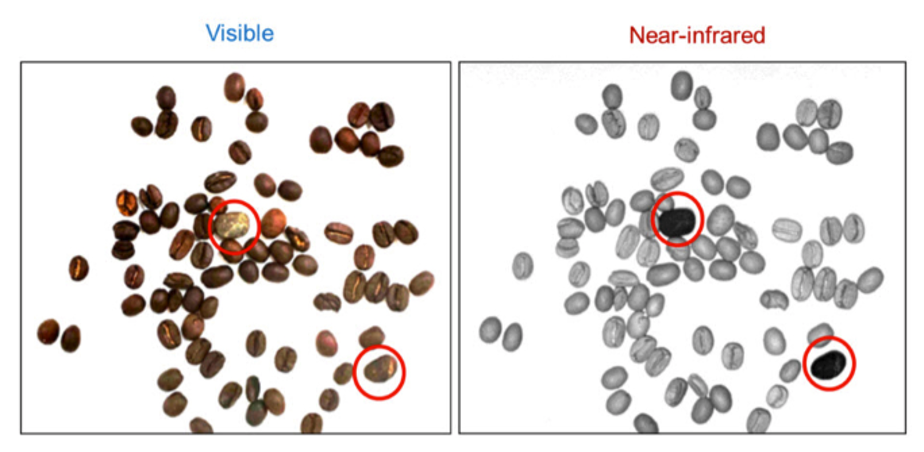
There are also major industrial demands for these cameras in quality inspection and control, especially in the food processing industry for inspection and detection of defects in goods. Certain plastics turn transparent in the SWIR range, and so VIS-SWIR cameras installed in food processing lines make it possible to detect defective products through plastic packaging. They also help to detect bruises in the agri-food industry. Bruises on fruit are filled with water, which is highly absorptive in the SWIR spectrum, and so the SWIR camera can easily detect the defect as a dark spot. Moreover, these cameras are quite useful when sorting out metal or stone impurities from food. For example, coffee beans and small stones can look alike when viewed under the visible light, but they drastically differ under SWIR light (Fig. 1).
2. Technology behind the current VIS-SWIR cameras
There are certain semiconductor materials that enable the existence of VIS-SWIR sensors. Conventional VIS range cameras all rely on silicon sensors with the sensitivity range of 300-1000 nm. The ability to detect the SWIR range beyond 1000 nm and up to 2500 nm normally requires certain epitaxially grown materials (Table 1). Usually, these materials are grown by atomic layer deposition at high temperatures and vacuum – a combination of conditions that make the sensor very expensive.
| Detector Material | Typical VIS-IR Detection Range | |
| Si | Silicon | 300 nm – 1.0 µm |
| InGaAs | Indium Gallium Arsenide | 900 nm – 1.7 µm |
| Ge | Germanium | 800 nm – 1.6 µm |
| PbS | Lead Sulfide | 1 µm – 2.8 µm |
| PbSe | Lead Selenide | 1 µm – 4.5 µm |
| InSb | Indium Antimonide | 2 µm – 5 µm |
| HgCdTe (MCT) | Mercury Cadmium Telluride | 2 µm – 14 µm |
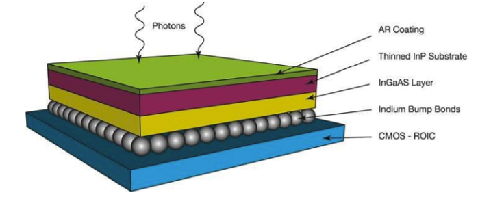
Currently, InGaAs technology is one of the dominant materials for SWIR detection. That is because it demonstrates the best efficiency in 900-1700 nm range: high special detectivity of D* up to 1 – 6 × 10¹³ Jones, high EQE (external quantum efficiency) of 70 %, and high responsivity. SWIR cameras based on InGaAs utilise a hybrid architecture that combines a silicon-based CMOS readout circuit with an InGaAs photosensitive array (Fig.2). The InGaAs device is normally grown on an indium phosphide (InP) substrate; its thickness and the ratio of indium (In) to gallium (Ga) will influence the wavelength sensitivity of the sensor. Each pixel of InGaAs array is connected with the pixel from silicon CMOS single read-out integrated circuit (ROIC) substrate via soldering bump bonds.
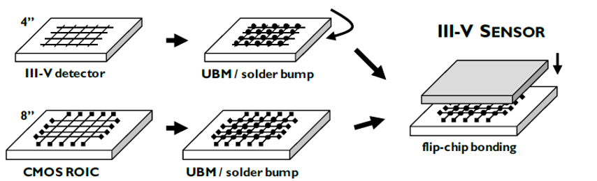
Combining the InGaAs array with the silicon CMOS readout circuit is a relatively complex and time-consuming process called “flip-chip hybridization”, requiring many manufacturing steps. First, the InGaAs sensors and silicon CMOS ROIC substrate are made separately. Then, solder bump is deposited in each pixel of both arrays. Finally, both arrays are combined with flip-chip bonding (Fig. 3). That multistep process results in a relatively low production yield and an increased price per unit. The current market price for a SWIR camera is between $5,000 and $30,000.
Despite this high cost, InGaAs sensors are far from being perfect. Currently, it is technically impossible to combine the readout circuit with the photosensitive area with 100 percent accuracy and uniformity. These sensors inevitably have a considerable percentage of defective pixels. Moreover, each pixel shows a slightly different behaviour. A raw image made by this camera looks noisy and requires defect-correction algorithms in the software.
Additional limitations include their relatively low resolution due to the large pixel size. The pixel size of the typical silicon CMOS sensor can be less than 1 um, bringing the camera resolution beyond 100 megapixels, whereas in hybrid InGaAs cameras, the pixel size is about 20-50 um, meaning that it gives a resolution which is 200-2,500 times lower (less than 0.5 megapixel). Although the resolution of VIS-SWIR cameras can be improved by using Cu-Cu connection bumps between the InGaAs and silicon CMOS ROIC substrate, to be able to reach a 5 um pixel size with 1.34-megapixel resolution, the photodetector fabrication cost is high and the operating SWIR spectral range is limited to less than 1700 nm.
Another drawback is that InGaAs technology has high noise level at room temperature and requires thermoelectric or cryogenic cooling to reduce the dark noise and the temperature dependent signal fluctuation.
3. Quantum dots make VIS-SWIR cameras affordable
The recent development of quantum dot technology has provided an excellent alternative to the InGaAs or other epitaxially grown materials, and has promised new opportunities for production of affordable broadband and high resolution VIS-SWIR cameras. Quantum dots (QDs), are small semiconducting nanoparticles, measuring just several nanometers in size, and they have outstanding photoluminescent and electroluminescent properties. In SWIR sensors, quantum dots serve as light absorbing layers that can convert light into an electrical signal (Fig. 4).

The distinguishing feature of quantum dots is that they can be deposited on top of the surface of the silicon CMOS ROIC substrate by a simple printing method. The printing is an affordable and convenient way of depositing NIR active material on top of the silicon substrate. It doesn’t require a high temperature, a vacuum or an expensive setup like the epitaxially grown materials do (Table 1). Moreover, the printing is a flexible technique which allows to deposit the material with any form, or dimensions, from small nanodroplets to large areas, all with high accuracy. This makes it possible to fabricate cost-efficient, high resolution SWIR cameras in a single read-out integrated circuit (ROIC) with broadband detection from 250 – 2500 nm (Fig.5). What is more, the pixel size can be as low as silicon CMOS pixels size. The process of creating a NIR camera becomes much simpler when utilising quantum dot technology.

Thanks to the easier printing process, high production scalability of silicon CMOS ROIC substrate, and low amount of quantum dots required per sensor, the price for quantum dot-based VIS-SWIR cameras is expected to be as low as $50 – $100 per unit. This is price is 100 times lower than that of InGaAs and Ge based sensors.
4. PbS (Lead Sulfide) quantum dots
There are several types of quantum dots that can work in NIR range: PbS, PbSe, InAs, InSb and HgTe Quantum Dots (Fig.6).
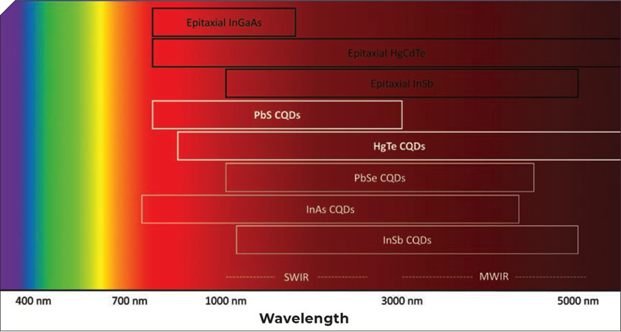
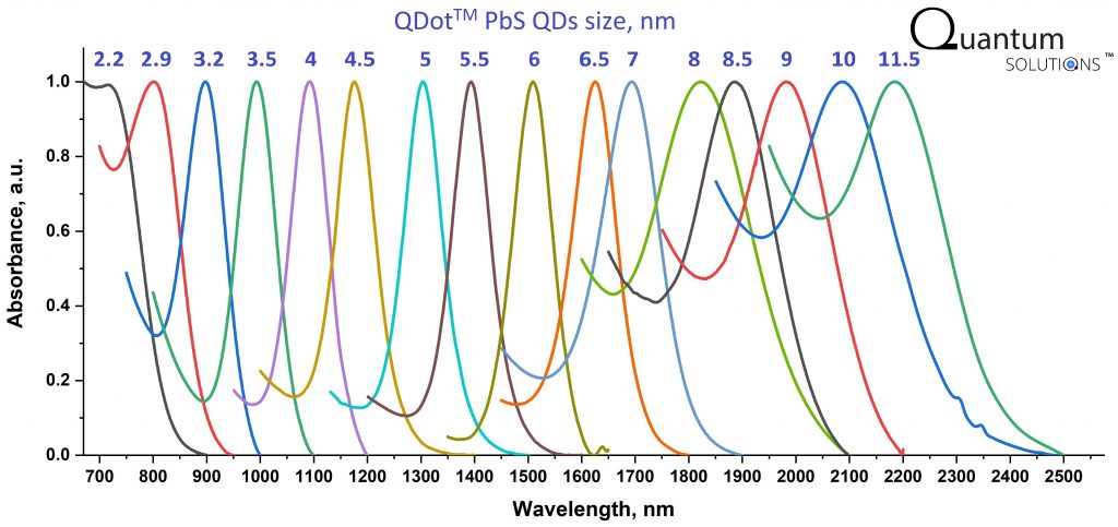
However, from an industrial application perspective the most appropriate material to use is PbS (Lead Sulfide) quantum dots, because of its high absorption coefficient, high photoelectric conversion and high tolerance to air. PbS QDs of different sizes can be synthesised with a tuneable bandgap from 1.5 eV to 0.5 eV, depending on the particle size (from 2 nm to 12 nm respectively). These dots have a absorption cut-off detectivity ranging from 800 nm to 2500 nm (Fig.7). These properties make PbS QDs preferable for fabricating and processing SWIR sensors.
Although PbS QDs might seem like a young technology, they have been proven to be reliable and a viable tool. It is worth noting that PbS in an epitaxially grown form (bulk, non-QD) has long been used in the field of NIR photodetectors within the sensitivity range of 1-3 um. For example, it is widely used in broadband spectrometers with SWIR range up to 2500 nm, such as the Agilent Cary 5000. As for PbS quantum dots, their first use in detectors was reported in academic articles in 2005, and since then they have drastically improved. PbS QDs are considered as progress from bulk PbS, as they have all the same features and then also additional advantages in terms of band gap tuneability, property changes by ligand engineering, printability and compatibility with silicon CMOS ROIC substrate.
Today, PbS QD based photodetectors’ responsivity (R) and special detectivity (D*) are high, with responsivity 103 – 105 A W-1 and an outstanding specific detectivity D* of 1011-1013 Jones. These values exceed those obtained with InGaAs-based photodetectors. Despite the relatively lower EQE (up to 30-50%) and long rise time (100 µs) when compared with InGaAs sensors, PbS QDs imagers show promise in the areas of high resolution and affordable VIS-SWIR cameras.
PbS QDs VIS-SWIR cameras have already been commercialised. One of the pioneers in the technology industrialisation is SWIR Vision System. They have introduced Acuros camera, which is also based on PbS Quantum Dots/Silicon CMOS technology and has a sensitivity range of 350-2000 nm. They supply cameras with various resolution 640*512 – 1920-180 (0.33 – 2.07 megapixels) with 15 um pixel size. SWIR Vision Systems quoted “Acuros™ CQD™ Full HD cameras deliver more than 6X the pixel resolution compared to InGaAs VGA cameras, delivering higher field-of-view and superior clarity to users with the need to resolve the finest details“.
Imec, an international research & development organisation, is another company that has been working on the development of PbS QDs SWIR cameras. According to their latest report, their silicon CMOS/PbS QDs camera has achieved a record high resolution, with pixel size of 1.82 um.and potential possibility to achieve over 20 megapixels. The efficiency of this camera is quite impressive: sensitivity variable between 400-2000 nm, EQE 20-60%, and special detectivity 1010 – 1013 Jones. Both Imec and SWIR Vision Systems integrate PbS QDs with silicon CMOS ROIC substrate that allow affordable broadband and high-resolution VIS-SWIR sensors.
PbS QDs high quality and production reproducibility are two of the most crucial requirements for industrial VIS-SWIR cameras, as they guarantee the reproducibility of camera parameters such as: sensitivity range, EQE, electrical gain and processability.
Quantum dots are a complex semiconductor nanomaterial consisting of the nanoparticle’s core and ligands surrounding the dots. Factors such as nanoparticles size dispersion, surface stoichiometric composition, facets and defect states, ligand nature and content all affect device performance. Therefore, to achieve high photoelectric gain, PbS QDs should meet specific criteria. First and foremost, quantum dots ought to be of a narrow size dispersion. Similar to deep traps, small band gap QDs can severely impede the extraction of photo carriers. Therefore, PbS QDs with size dispersion greater than 20% are limited in their application in photodetectors. Secondly, in order to minimise trap states, limiting the sensor efficiency, the surface of the QDs needs to be defect-free. It is extremely important that QDs are synthesised in a controlled environment, following strict growth and cleaning synthesis procedures. Thirdly, proper ligand types and content should be selected. Summing up, PbS quantum dots should be of a high optoelectronic grade quality with batch to batch reproducibility in order to be useful for industrial VIS-SWIR cameras.
In conclusion, VIS-SWIR cameras with PbS QDs have the potential to be high resolution and affordable, and there is a huge demand this kind of product in areas such as quality inspection and control, security CCTV cameras, automotive and mobile cameras. Quantum dot technology can help to extend the current sensitivity of silicon cameras from the limited VIS range (300-1000 nm) to create more advantageous VIS-SWIR cameras with a range of (300-2500 nm).
5. About Quantum Solutions
Quantum Solutions is a nanotechnology company and the leader in providing reliable Quantum dots for VIS-SWIR cameras. Quantum Solutions is able to accommodate the strict requirements of the optoelectronic industry. Our QDot™ PbS Quantum Dots have high optoelectronic grade quality and precise batch to batch production reproducibility, which supports the supply of materials for VIS-SWIR cameras from small to large industrial scales. Quantum Solutions proprietary manufacturing technology makes it possible to produce the whole range of PbS quantum dots with tuneable wavelengths from 900 – 2500 nm absorption profiles with high reproducibility of the absorbance peak as low as ±5 nm for customised cameras needs. They have extremely narrow size dispersion < 5-10 %, with low defect surfaces and controllable ligand content. Contact us [email protected] to discuss your needs in building the next generation VIS-SWIR camera with quantum dot technology.
6. Useful links:
- https://www.photonics.com/Articles/Graphene-CMOS_High-Res_Sensor_Images_Visible_and/a62111#
- https://www.youtube.com/watch?v=cmo4IvNDs2g
- https://www.youtube.com/watch?v=mS4EBbALAFM
- https://hub.hamamatsu.com/us/en/ask-engineer/nir-and-swir-questions-and-answers/index.html
- https://www.horiba.com/en_en/technology/spectroscopy/detectors/detectors/
- https://www.degruyter.com/document/doi/10.1515/nanoph-2017-0061/html
- https://www.photonics.com/Articles/SWIR_Applications_and_Challenges_A_Primer/a56646#
- https://qd-uki.co.uk/wp-content/uploads/sites/2/2020/01/Ninox-White-Paper-Final.pdf
- https://www.princetoninstruments.com/learn/camera-fundamentals/ingaas-sensors-the-basics
- https://www.mdpi.com/1424-8220/17/12/2867
- https://semiengineering.com/scaling-cmos-image-sensors/#
- https://www.eenewseurope.com/news/sensor-megapixel-visible-swir
- https://quantum-solutions.com/blog/quantum-dots/
- https://onlinelibrary.wiley.com/doi/full/10.1002/msid.1165
- https://www.lasercomponents.com/de-en/product/pbs-detectors/
- https://www.nature.com/articles/nmat1299
- https://www.swirvisionsystems.com/acuros-swir-camera/
- https://spectrum.ieee.org/consumer-electronics/audiovideo/move-over-cmos-here-come-snapshots-by-quantum-dots
- https://www.24-7pressrelease.com/press-release/474881/swir-vision-systems-introduces-first-commercial-full-hd-eswir-cameras
- https://image-sensors-world.blogspot.com/2020/12/imec-presents-thin-film-swir-sensor.html
- https://pubs.rsc.org/en/content/articlelanding/2021/tc/d0tc04612d#!divAbstract
- https://quantum-solutions.com/
- https://quantum-solutions.com/product/qdot-lead-sulfide-pbs-quantum-dots/