Q.Dot™ InAs quantum dot n-type ink
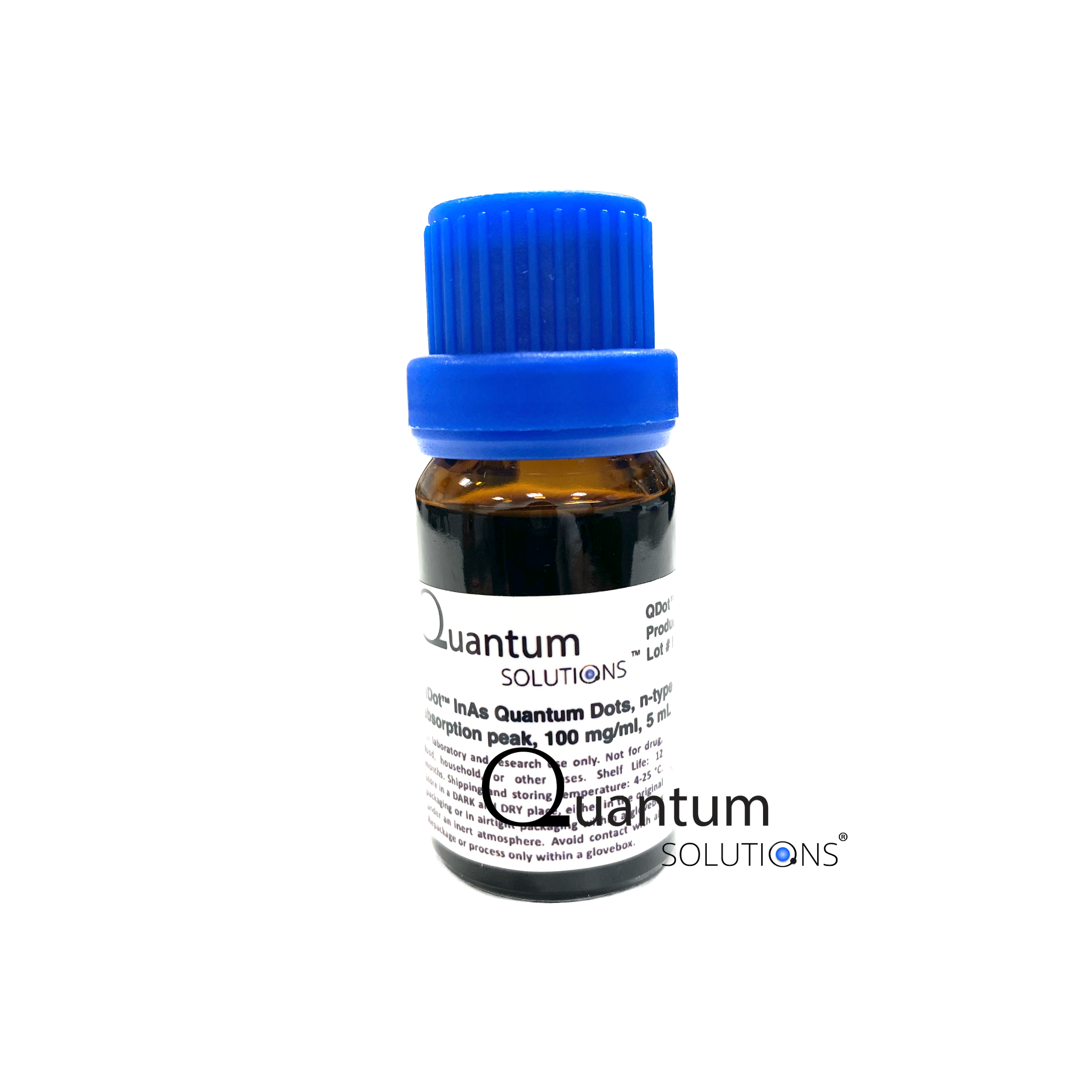
Quantum Solutions provides the Q.Dot™ InAs quantum dot n-type ink (n-ink), specifically designed for the fabrication of highly efficient SWIR (short-wave infrared) photodiodes and image sensors. The n-ink is negatively doped, meaning the work function of thin films is close to the conduction band of the material. Q.Dot™ InAs quantum dot n-ink offers multiple advantages. Firstly, it eliminates the need for complex solid ligand exchange procedures. Secondly, it enables the straightforward creation of a thick and smooth quantum dot absorber layer, up to 100 nm, which can be effortlessly deposited onto a substrate using spin-coating or other solution processing methods. Multiple layer deposition is possible to achieve the desired thickness of 200–400 nm. Furthermore, Q.Dot™ InAs quantum dot n-ink delivers exceptional cost-efficiency, with only 5 mL required to coat one layer on a large 200 mm wafer, making it an ideal choice for scaling up production processes in SWIR photodiodes and image sensors.


Quantum Solutions offers a range of materials for fabricating the Q.Dot™ photodiode stack, which can be used in sensing and imaging applications. The principal device structure comprises several thin layers, referred to as the Q.Dot™ stack, placed on top of a substrate. Working from the bottom up, the structure includes a bottom electrode, HTL (hole transporting layer), quantum dots absorber, ETL (electron transporting layer), and transparent top electrode.
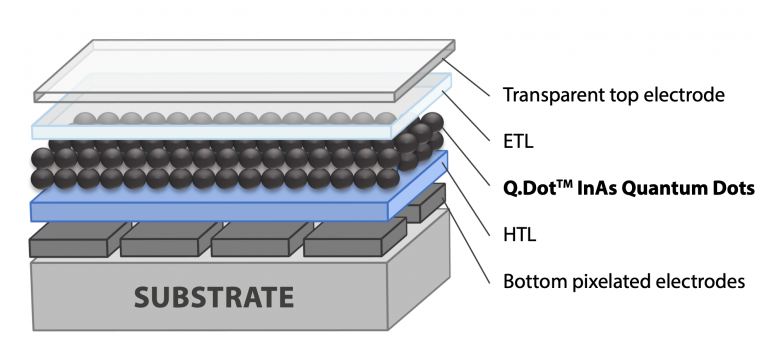
Q.Dot™ stack materials, including HTL, quantum dots, and ETL, can be deposited from solution onto any target substrate, such as glass, silicon, or a ROIC platform, using spin-coating methods. These novel solution-based methods for manufacturing thin films of compound semiconductor materials have made it possible to create artificial nanocrystalline structures that offer unprecedented possibilities. Unlike epitaxial layers, the quality of quantum-dot semiconductors is less dependent on the crystallographic characteristics of substrates and their interfacial relationships. Solution-based methods provide flexibility and broad material choice for specialised carrier transport layers enabling tuneable photodiode functions.
Quantum Solutions provides the Q.Dot™ InAs quantum dot n-type ink (n-ink), specifically designed for the fabrication of highly efficient SWIR (short-wave infrared) photodiodes and image sensors. The n-ink is negatively doped, which means the work function of thin films is close to the conduction band of the material. Q.Dot™ InAs quantum dot n-ink provides several advantages. Firstly, it eliminates the need for complex solid ligand exchange procedures. Secondly, it enables the straightforward creation of a thick and smooth quantum dot absorber layer, up to 100 nm. This layer can be effortlessly deposited onto a substrate using techniques such as spin-coating or other solution processing methods. Multiple layer deposition is possible to achieve the desired thickness of 200–400 nm. Furthermore, Q.Dot™ InAs quantum dot n-ink offers exceptional cost-efficiency in terms of ink consumption. Only 5 mL of this ink are required to coat one layer on a large 200 mm wafer, making it a practical choice for scaling up production processes in the field of SWIR photodiodes and image sensors.
Q.Dot™ InAs Quantum Dot n-type ink offers the following features:
-
Efficient solution-processed photoelectric absorber nanomaterial for use in short-wave infrared (SWIR) photodetectors and image sensors.
-
Simple one-step deposition on substrates (CMOS wafers, silicon, or glass wafers) by spin-coating processes, forming a thick (80–100 nm) quantum dot absorber layer. No ligand exchange process required. Multiple layers deposition is possible to achieve the desired thickness of 200–400 nm.
-
Extremely economical material consumption, with 5 mL being sufficient for coating one layer on a large 200 mm wafer.
-
A wide range of product availability from 3 to 8.5 nm of quantum dot size, covering the absorbance cut-off from 900 nm to 1750 nm.
-
Narrow particle size distribution (STDV < 5–10%) for the formation of a compact and defect-free quantum dot absorber layer.
Click here to view the Technical Specification for detailed information.
Q.Dot™ is a trademark of QUANTUM SOLUTIONS. Contact us to make any requests and questions or buy products online
