QDot™ InAs Quantum Dots, fatty acid capped

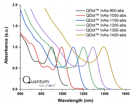
QDot™ InAs (Indium Arsenide) Quantum Dots absorb light from UV and visible up to the short-wave infrared (SWIR) spectral range. The absorption cut-off profiles can be tuned from 900 to 1600 nm simply by changing the nanoparticle sizes from 3 to 7 nm. This material has outstanding light absorption and photoelectrical properties and is considered the best lead-free quantum dot absorber in SWIR photodetectors and image sensors. Novel solution-based methods for depositing thin films of these quantum dots have made it possible to create artificial nanocrystalline InAs absorbing structures at affordable cost that offer unprecedented possibilities. Unlike epitaxially grown InAs or InGaAs thin films, QDot™ InAs quantum dots can be deposited within a QDot™ photodiode stack using spin-coating methods from a colloidal solution. In principle, a QDot™ photodiode stack consists of a substrate, an HTL (hole transport layer), a QDot™ InAs Quantum Dots absorber, an ETL (electron transport layer), and a transparent top electrode.
QDot™ InAs (Indium Arsenide) Quantum Dots absorb light from UV and visible up to the short-wave infrared (SWIR) spectral range. The absorption cut-off profiles can be tuned from 900 to 1600 nm simply by changing the nanoparticle sizes from 3 to 7 nm. This material has outstanding light absorption and photoelectrical properties and is considered the best lead-free quantum dot absorber in short-wave infrared (SWIR) photodetectors and image sensors.

QDot™ InAs quantum dots can be deposited within a QDot™ photodiode stack using spin-coating methods from a colloidal solution. In principle, a QDot™ photodiode stack consists of a substrate, an HTL (hole transport layer), a QDot™ InAs Quantum Dots absorber, an ETL (electron transport layer), and a transparent top electrode.
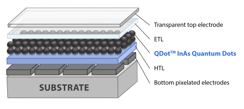
These novel solution-based methods for depositing thin films of compound semiconductor materials have made it possible to create artificial nanocrystalline InAs absorbing structures at affordable cost that offer unprecedented possibilities. Unlike epitaxially grown InAs or InGaAs thin films, QDot™ InAs quantum dots can be deposited within a QDot™ photodiode stack using spin-coating methods from a colloidal solution. In principle, a QDot™ photodiode stack consists of a substrate, an HTL (hole transport layer), a QDot™ InAs Quantum Dots absorber, an ETL (electron transport layer), and a transparent top electrode. the quality of quantum dot semiconductors is less dependent on the crystallographic characteristics of substrates and their interfacial relationships ensuring the device architecture flexibility and large-scale manufacturability on 8’’ or 12’’ wafers.
QDot™ InAs Quantum Dots offer the following advantages:
- Solution-processed compound semiconductor nanomaterial to be used in short-wave infrared (SWIR)/near-infrared (NIR) photodetectors and image sensors.
- Easy integration within a QDot™ photodiode stack through spin-coating or other printing processes, guaranteeing affordability and manufacturability on large 8’’ or 12’’ wafers.
- Lead-free and RoHS compliant, freely usable in consumer electronics, automotive, and machine vision applications.
- Fast decay time in the nanosecond range, opening up applications for Time-of-Flight (ToF) and LiDAR applications.
Click here to view the Technical Specification for detailed information.
QDot™ is a trademark of QUANTUM SOLUTIONS. Contact us to make any requests and questions or buy products online